1. Please upload the Gerber & BOM Files and board making instructions
2. The uploaded file format supports ZIP, RAR, 7Z compression package, less than 50MB
1. Please upload the Gerber Files and board making instructions
1. Please upload the BOM Files
Discover bqpwb’s RF antenna PCB, engineered for superior performance in radio frequency applications. Our PCBs are designed to enhance signal quality and reliability, offering optimal solutions for RF and antenna technologies.
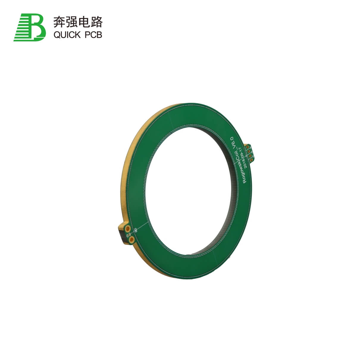
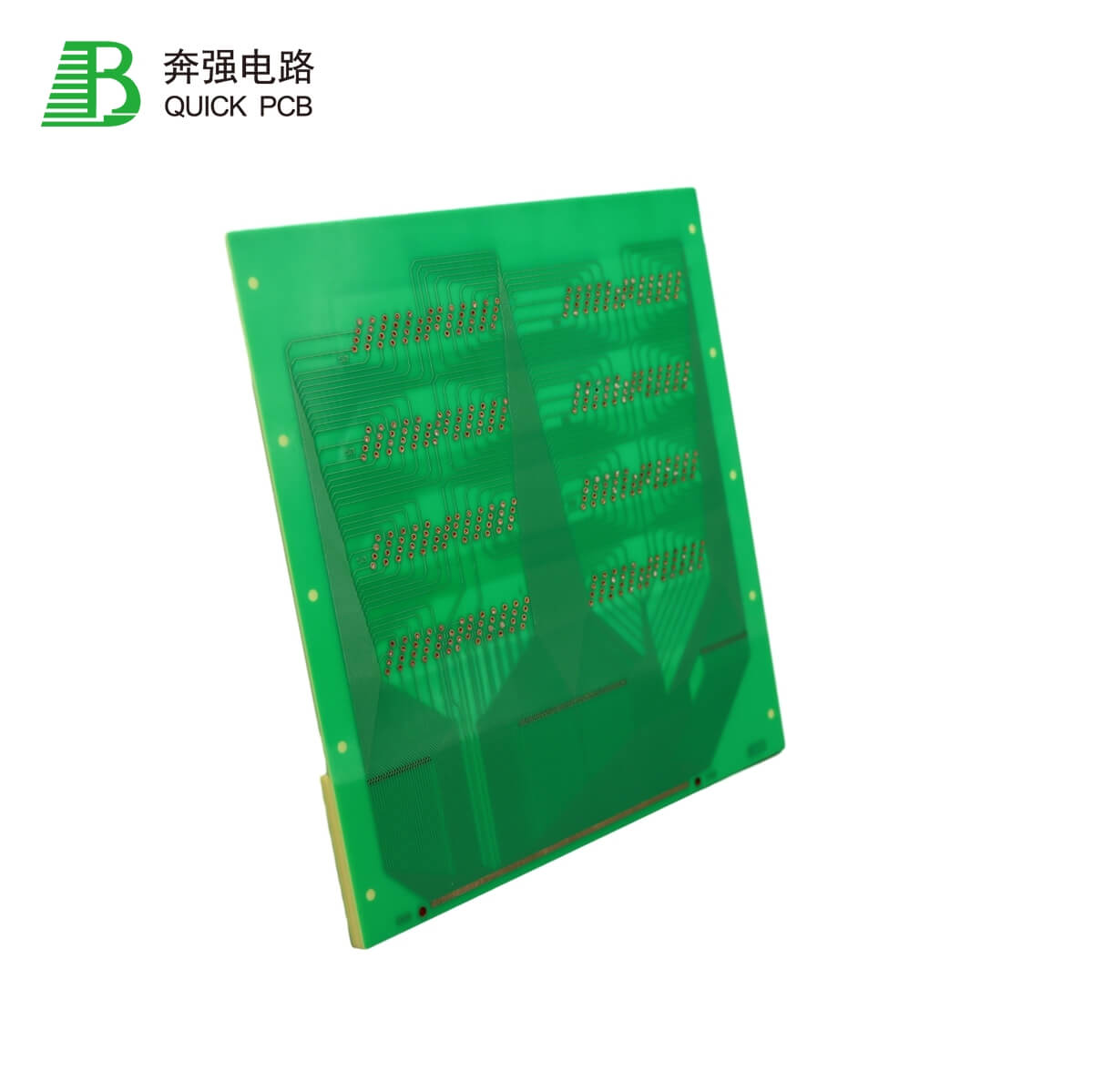
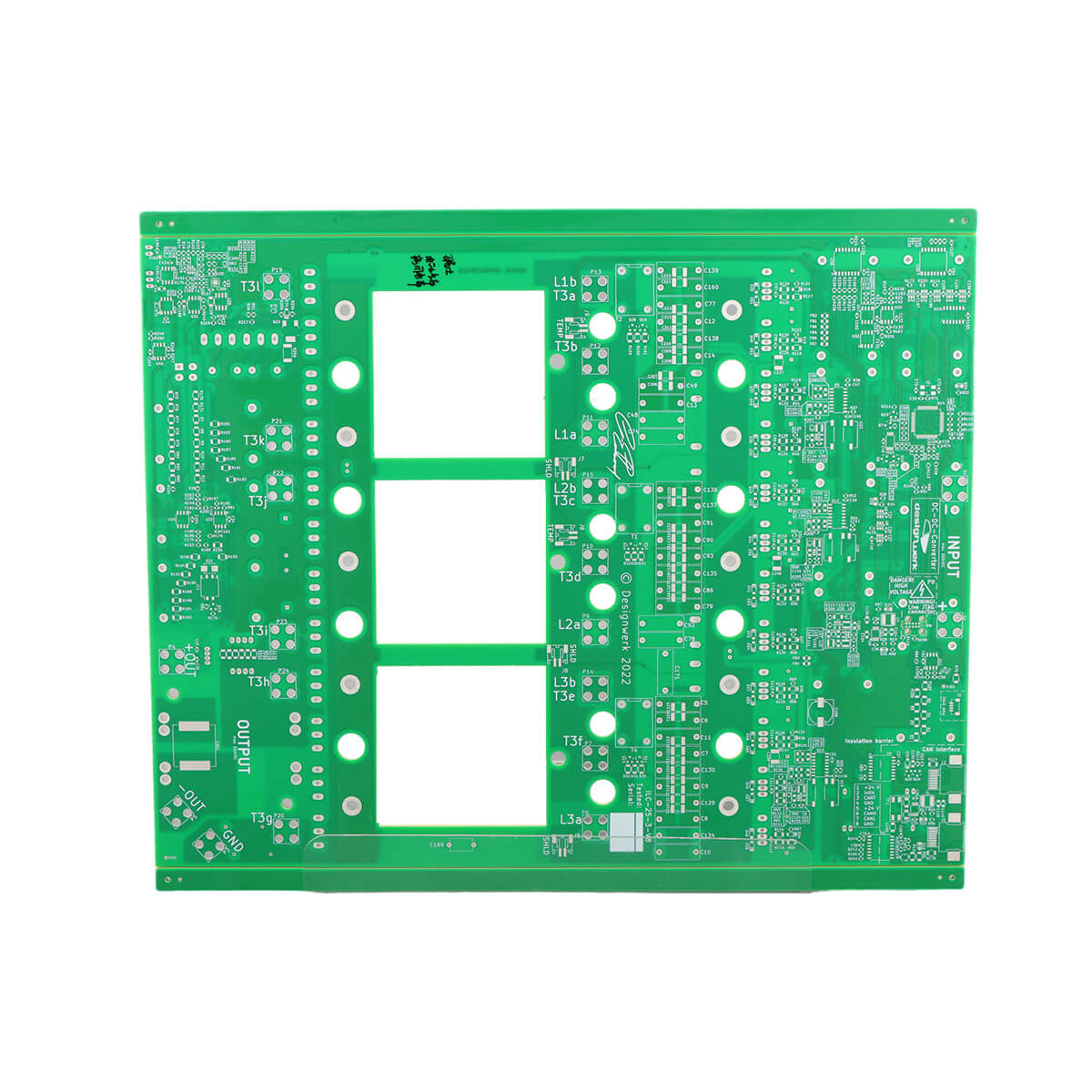
14 layers HDI Copper thickness inside and outside: 2 OZ Coil plate Mechanical blind holes + Drill control Thickness of board: 3.3 mm
Product Details
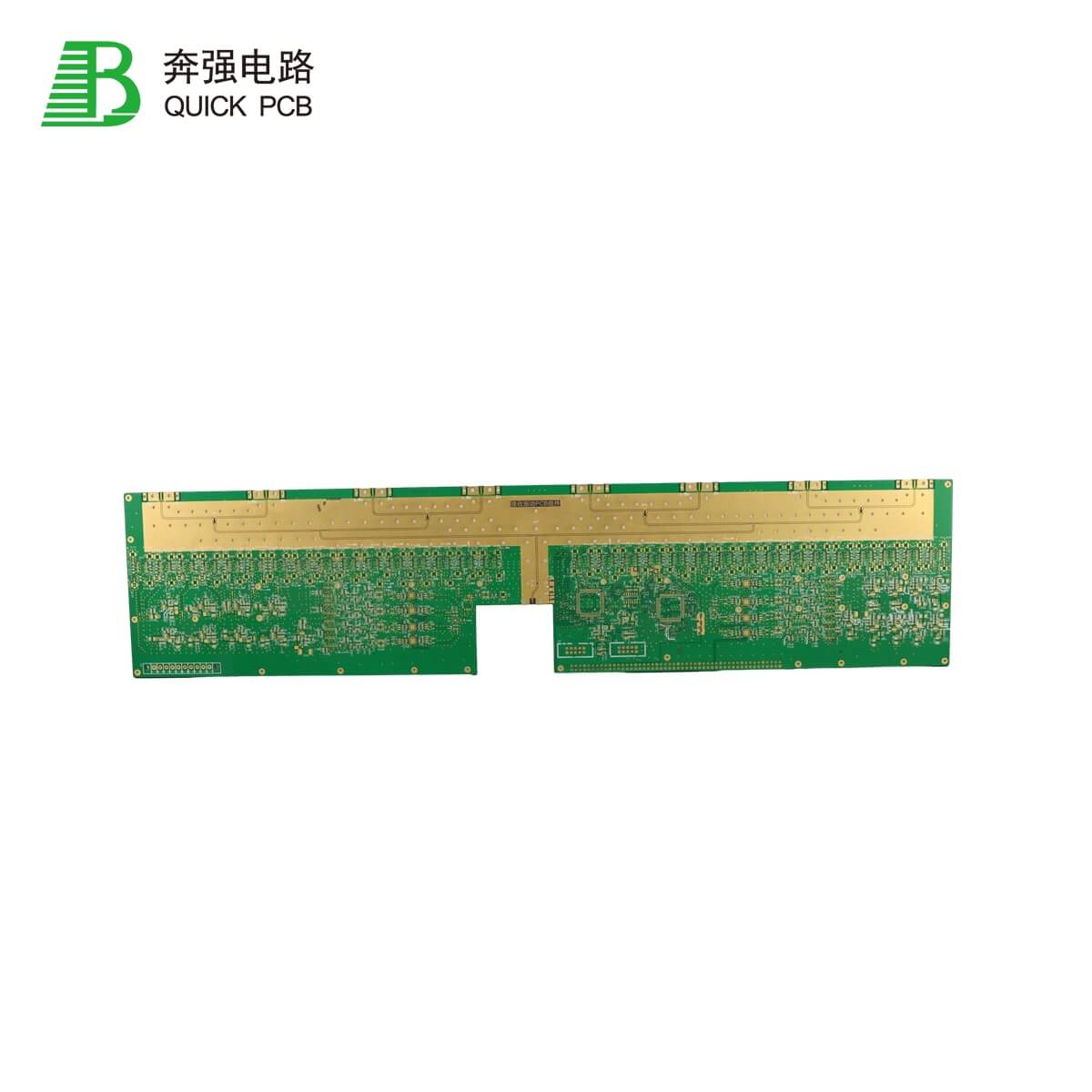
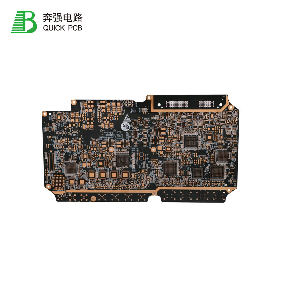
Step Golden Finger Board Material: S1000-2M 8 layers 1-step HDI 1+N+1 HDI Surface Finish: ENIG + Gold finger
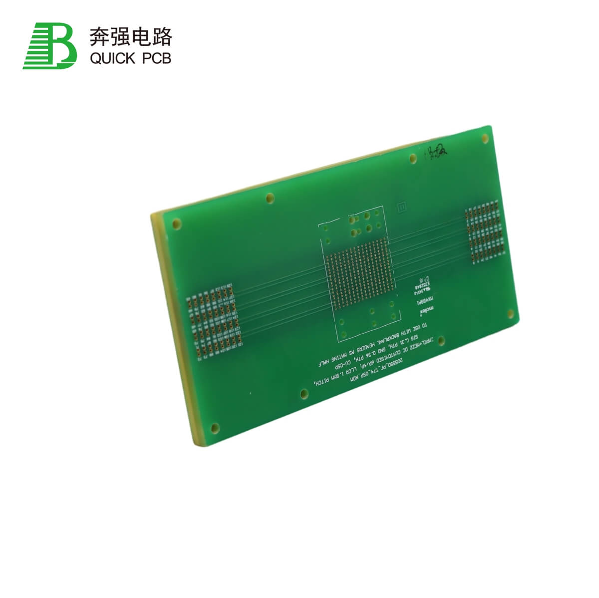
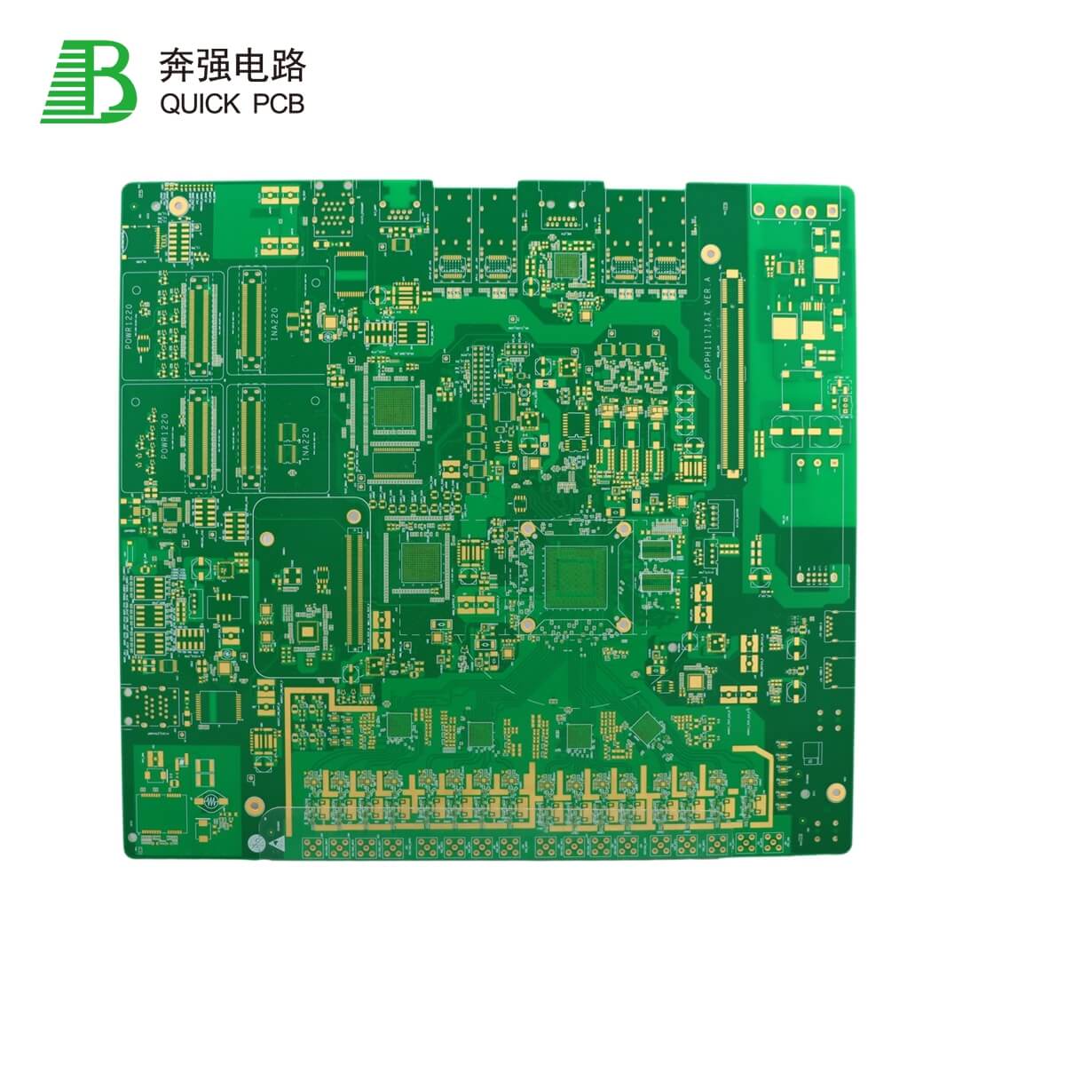
Application Characteristic Material Layer Communication High speed+high TG material IT968TC+Shengyi S1000-2M 10L Thickness Min hole diameter Min width/space Internal Number 1.00.1mm Laser hole: 0.10mm, Mechanical hole 0.15mm 100/100um S221021G10 Surface f
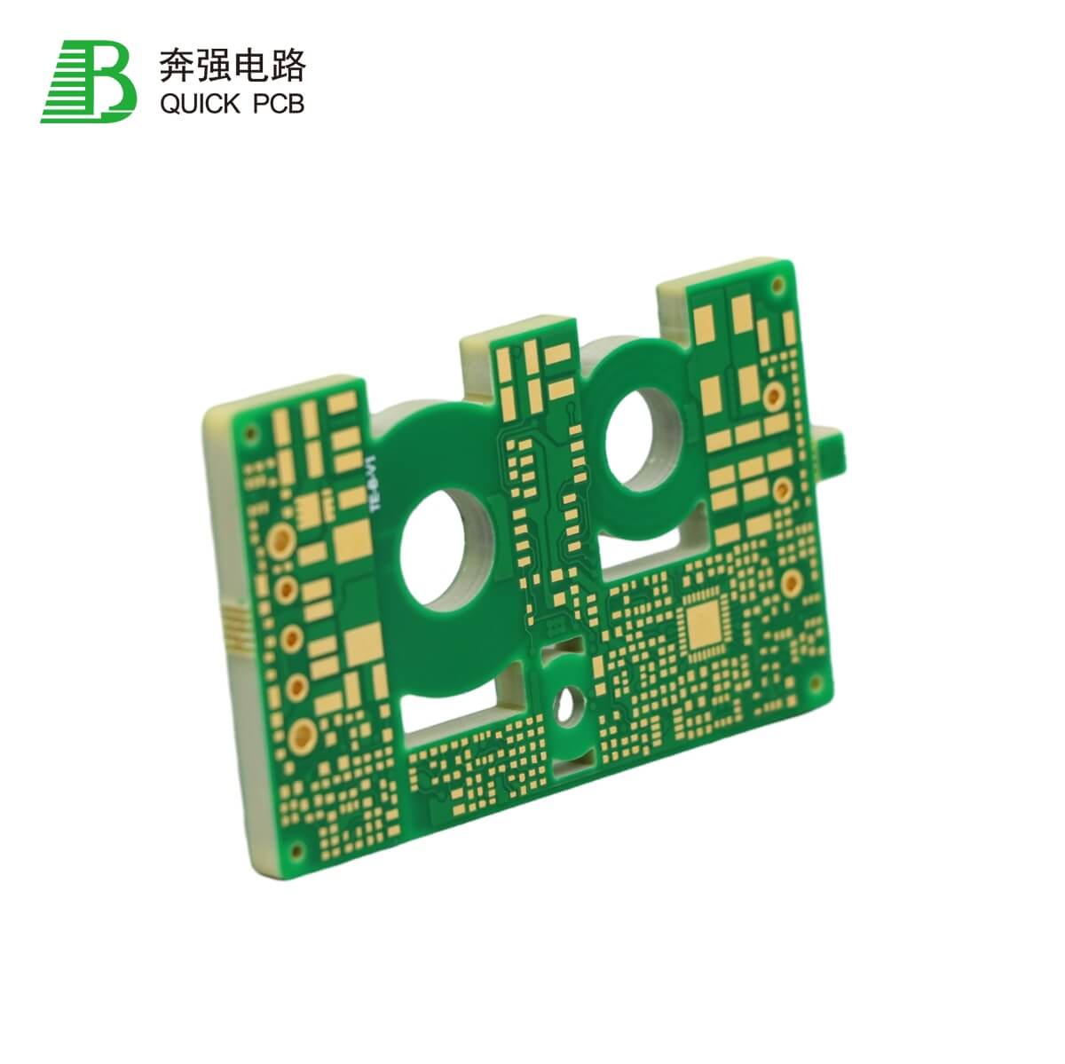
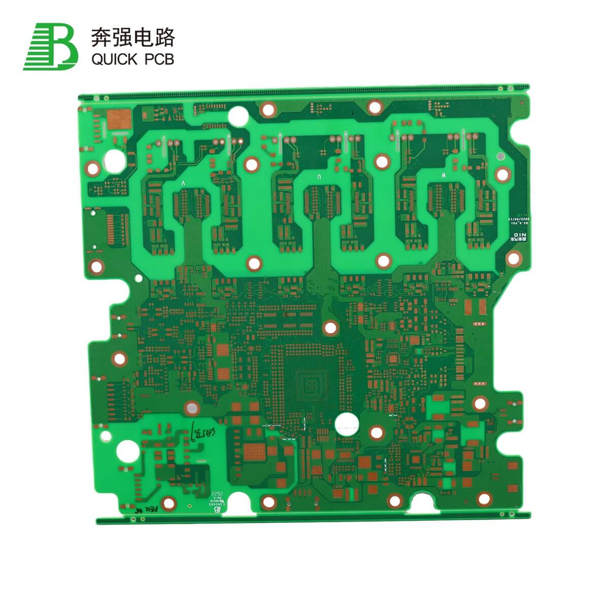
Customs Security Area RO5880 + FR-4 mixed pressure 14 layers Mechanical blind holes Thickness of board: 3.2 mm
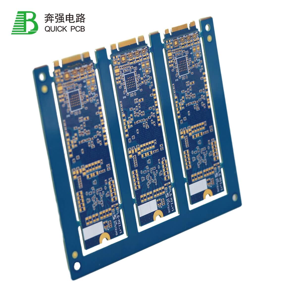
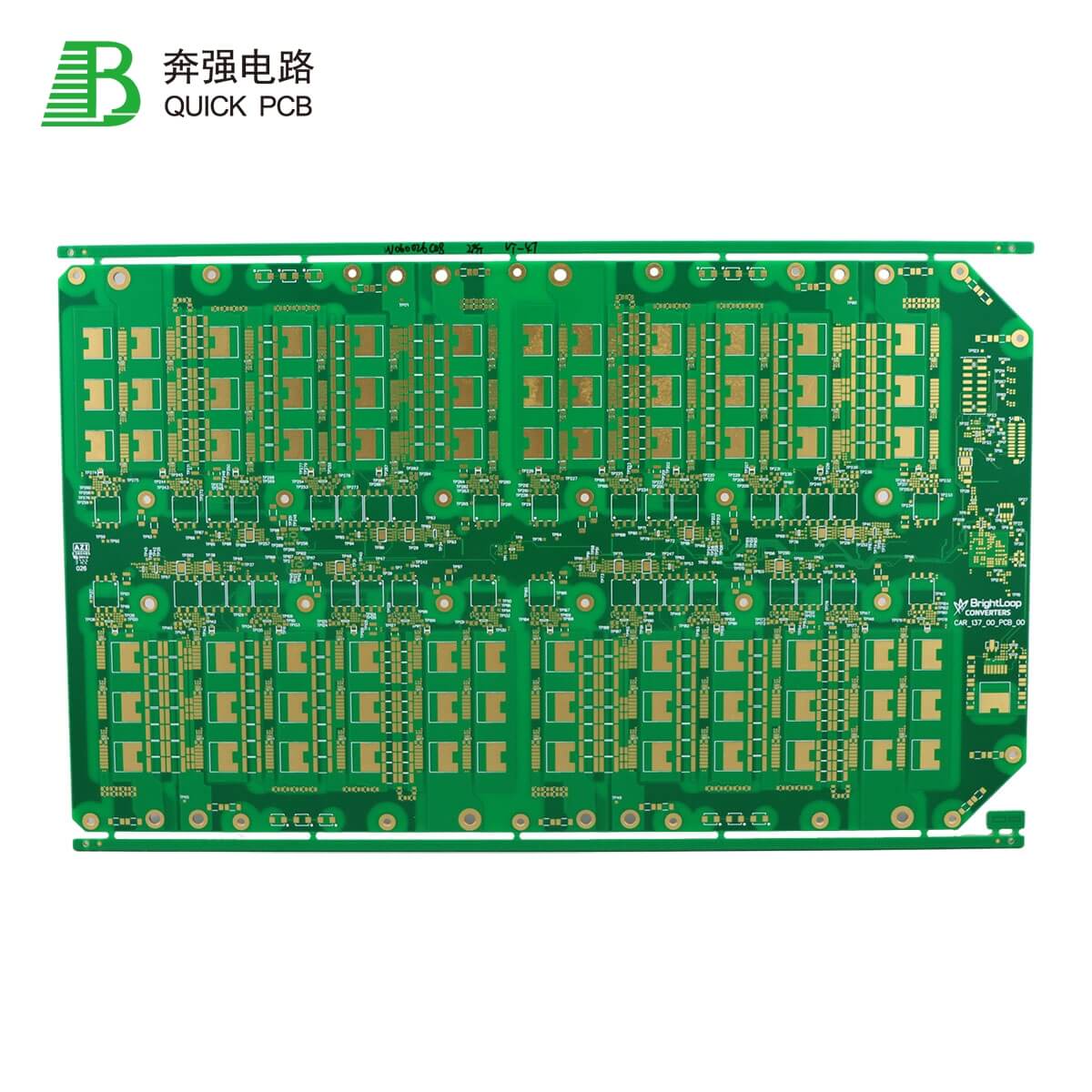
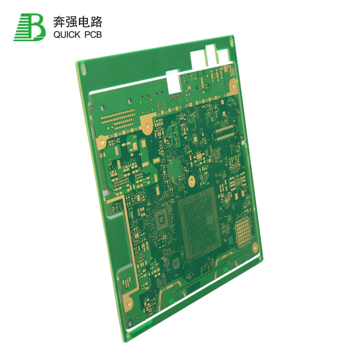
Computer Field 12 layers Backdrilling processes Aspect ratio: 10:1 Back drill
sales@bqpwb.com
https://linkedin.com/company/quickpcb